- 您现在的位置:买卖IC网 > Sheet目录327 > HW-V5-ML555-G (Xilinx Inc)BOARD EVAL FOR VIRTEX-5 ML555
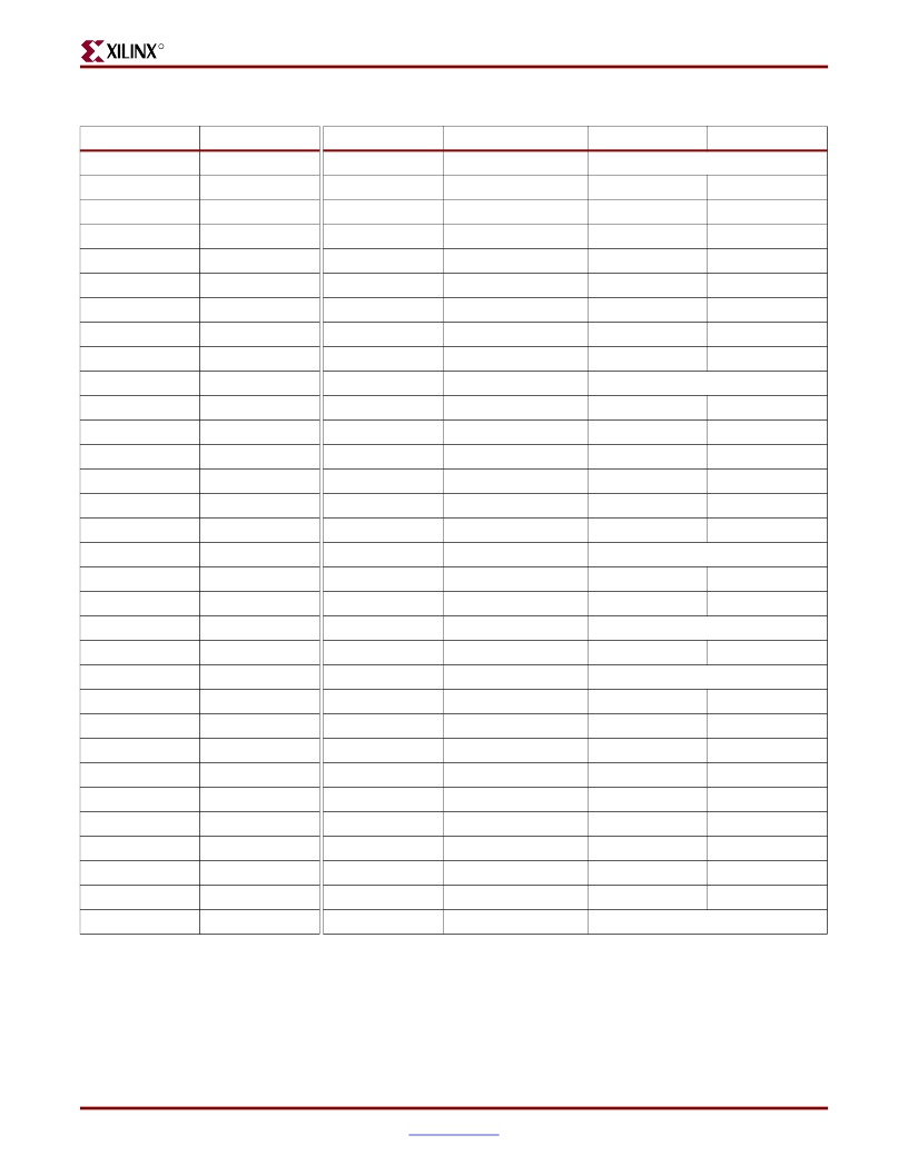
Table 3-11:
R
Ethernet PHY Daughtercard J16 Connection
Ethernet PHY Daughtercard Support
J16-EVEN
2
4
6
8
10
12
14
16
18
20
22
24
26
28
30
32
34
36
38
40
42
44
46
48
50
52
54
56
58
60
62
64
Signal
GND
GND
GND
GND
GND
GND
GND
GND
GND
GND
GND
GND
GND
GND
GND
GND
GND
GND
GND
GND
GND
GND
GND
GND
GND
GND
GND
GND
GND
GND
GND
GND
J16-ODD
1
3
5
7
9
11
13
15
17
19
21
23
25
27
29
31
33
35
37
39
41
43
45
47
49
51
53
55
57
59
61
63
Signal
No connect
P1_RXC_RXCLK (3)
P1_RD_RXD1
P1_RXCTL_RXDV
P1_RCLK1 (4)
P1_CRS
P1_RXER
P1_RXD7
P1_RD_RXD0
No connect
P1_RD_RXD2
P1_RD_RXD3
P1_RXD4
P1_RXD5
P1_RXD6
P0_CRS
No connect
P0_RD_RXD0
P0_RD_RXD1
No connect
P0_RD_RXD2
No connect
P0_RXCTL_RXDV
P0_RXD4
P0_RXD5
P0_RXD6
P0_RXD7
P0_RCLK1 (4)
P0_RD_RXD3
P0_RXER
P0_RXC_RXCLK (3)
No connect
FPGA Pin (1)
J10
E11
M10
K18
G11
G12
E6
T9
G6
T10
F5
R9
H5
R11
M6
N8
M7
J6
P5
L5
P6
K6
H14
J5
R8
H7
NC (2)
NC
NC
NC
NC
NC
FPGA In/Out
In
In
In
In
In
In
In
In
In
In
In
In
In
In
In
In
In
In
In
In
In
In
In
In
In
In
Notes:
1. These signals are connected to FPGA banks 12 and 20. The bank reference voltage, V CCO , is 2.5V. See the ML555 board schematics
on the CD-ROM for additional information.
2. NC = no connect.
3. These clocks are connected to FPGA clock-capable I/O pins.
4. These clocks are connected to FPGA global clock pins.
Virtex-5 FPGA ML555 Development Kit
UG201 (v1.4) March 10, 2008
43
发布紧急采购,3分钟左右您将得到回复。
相关PDF资料
HW-V5-ML561-UNI-G
EVALUATION PLATFORM VIRTEX-5
I-JET
JTAG ARM DEBUGGING PROBE
IAC24A
INPUT MODULE AC 5MA 24VDC
IAC5EQ
INPUT MODULE AC 10MA 5VDC
IB8RM
SURGE SUPP 8OUT 12'CORD W/REMOTE
IBAR12-20T
SURGE SUPPRSSR 20A 12OUT RACKMNT
IBAR12/20ULTRA
SURGE SUPPRSSR 20A 12OUT RACKMNT
IBAR12ULTRA
SURGE SUPPRSSR 15A 12OUT RACKMNT
相关代理商/技术参数
HW-V5-ML555-G-PROMO1
功能描述:BOARD EVAL FOR VIRTEX-5 ML505 RoHS:是 类别:编程器,开发系统 >> 过时/停产零件编号 系列:- 标准包装:1 系列:- 传感器类型:CMOS 成像,彩色(RGB) 传感范围:WVGA 接口:I²C 灵敏度:60 fps 电源电压:5.7 V ~ 6.3 V 嵌入式:否 已供物品:成像器板 已用 IC / 零件:KAC-00401 相关产品:4H2099-ND - SENSOR IMAGE WVGA COLOR 48-PQFP4H2094-ND - SENSOR IMAGE WVGA MONO 48-PQFP
HW-V5-ML561-UNI-G
功能描述:EVALUATION PLATFORM VIRTEX-5 RoHS:是 类别:编程器,开发系统 >> 通用嵌入式开发板和套件(MCU、DSP、FPGA、CPLD等) 系列:Virtex®-5 LXT 产品培训模块:Blackfin® Processor Core Architecture Overview
Blackfin® Device Drivers
Blackfin® Optimizations for Performance and Power Consumption
Blackfin® System Services 特色产品:Blackfin? BF50x Series Processors 标准包装:1 系列:Blackfin® 类型:DSP 适用于相关产品:ADSP-BF548 所含物品:板,软件,4x4 键盘,光学拨轮,QVGA 触摸屏 LCD 和 40G 硬盘 配用:ADZS-BFBLUET-EZEXT-ND - EZ-EXTENDER DAUGHTERBOARDADZS-BFLLCD-EZEXT-ND - BOARD EXT LANDSCAP LCD INTERFACE 相关产品:ADSP-BF542BBCZ-4A-ND - IC DSP 16BIT 400MHZ 400CSBGAADSP-BF544MBBCZ-5M-ND - IC DSP 16BIT 533MHZ MDDR 400CBGAADSP-BF542MBBCZ-5M-ND - IC DSP 16BIT 533MHZ MDDR 400CBGAADSP-BF542KBCZ-6A-ND - IC DSP 16BIT 600MHZ 400CSBGAADSP-BF547MBBCZ-5M-ND - IC DSP 16BIT 533MHZ MDDR 400CBGAADSP-BF548BBCZ-5A-ND - IC DSP 16BIT 533MHZ 400CSBGAADSP-BF547BBCZ-5A-ND - IC DSP 16BIT 533MHZ 400CSBGAADSP-BF544BBCZ-5A-ND - IC DSP 16BIT 533MHZ 400CSBGAADSP-BF542BBCZ-5A-ND - IC DSP 16BIT 533MHZ 400CSBGA
HW-V5-ML561-UNI-G-J
功能描述:EVALUATION PLATFORM VIRTEX-5 RoHS:是 类别:编程器,开发系统 >> 通用嵌入式开发板和套件(MCU、DSP、FPGA、CPLD等) 系列:Virtex®-5 LXT 产品培训模块:Blackfin® Processor Core Architecture Overview
Blackfin® Device Drivers
Blackfin® Optimizations for Performance and Power Consumption
Blackfin® System Services 特色产品:Blackfin? BF50x Series Processors 标准包装:1 系列:Blackfin® 类型:DSP 适用于相关产品:ADSP-BF548 所含物品:板,软件,4x4 键盘,光学拨轮,QVGA 触摸屏 LCD 和 40G 硬盘 配用:ADZS-BFBLUET-EZEXT-ND - EZ-EXTENDER DAUGHTERBOARDADZS-BFLLCD-EZEXT-ND - BOARD EXT LANDSCAP LCD INTERFACE 相关产品:ADSP-BF542BBCZ-4A-ND - IC DSP 16BIT 400MHZ 400CSBGAADSP-BF544MBBCZ-5M-ND - IC DSP 16BIT 533MHZ MDDR 400CBGAADSP-BF542MBBCZ-5M-ND - IC DSP 16BIT 533MHZ MDDR 400CBGAADSP-BF542KBCZ-6A-ND - IC DSP 16BIT 600MHZ 400CSBGAADSP-BF547MBBCZ-5M-ND - IC DSP 16BIT 533MHZ MDDR 400CBGAADSP-BF548BBCZ-5A-ND - IC DSP 16BIT 533MHZ 400CSBGAADSP-BF547BBCZ-5A-ND - IC DSP 16BIT 533MHZ 400CSBGAADSP-BF544BBCZ-5A-ND - IC DSP 16BIT 533MHZ 400CSBGAADSP-BF542BBCZ-5A-ND - IC DSP 16BIT 533MHZ 400CSBGA
HW-V5-PCIE2-UNI-G
功能描述:KIT DEV PCIEXPRESS GTX VIRTEX5 RoHS:是 类别:编程器,开发系统 >> 通用嵌入式开发板和套件(MCU、DSP、FPGA、CPLD等) 系列:Virtex® -5 产品培训模块:Blackfin® Processor Core Architecture Overview
Blackfin® Device Drivers
Blackfin® Optimizations for Performance and Power Consumption
Blackfin® System Services 特色产品:Blackfin? BF50x Series Processors 标准包装:1 系列:Blackfin® 类型:DSP 适用于相关产品:ADSP-BF548 所含物品:板,软件,4x4 键盘,光学拨轮,QVGA 触摸屏 LCD 和 40G 硬盘 配用:ADZS-BFBLUET-EZEXT-ND - EZ-EXTENDER DAUGHTERBOARDADZS-BFLLCD-EZEXT-ND - BOARD EXT LANDSCAP LCD INTERFACE 相关产品:ADSP-BF542BBCZ-4A-ND - IC DSP 16BIT 400MHZ 400CSBGAADSP-BF544MBBCZ-5M-ND - IC DSP 16BIT 533MHZ MDDR 400CBGAADSP-BF542MBBCZ-5M-ND - IC DSP 16BIT 533MHZ MDDR 400CBGAADSP-BF542KBCZ-6A-ND - IC DSP 16BIT 600MHZ 400CSBGAADSP-BF547MBBCZ-5M-ND - IC DSP 16BIT 533MHZ MDDR 400CBGAADSP-BF548BBCZ-5A-ND - IC DSP 16BIT 533MHZ 400CSBGAADSP-BF547BBCZ-5A-ND - IC DSP 16BIT 533MHZ 400CSBGAADSP-BF544BBCZ-5A-ND - IC DSP 16BIT 533MHZ 400CSBGAADSP-BF542BBCZ-5A-ND - IC DSP 16BIT 533MHZ 400CSBGA
HW-VID-KIT
功能描述:可编程逻辑 IC 开发工具 Lattice Video Interface Kit
RoHS:否 制造商:Altera Corporation 产品:Development Kits 类型:FPGA 工具用于评估:5CEFA7F3 接口类型: 工作电源电压:
HW-VL1
制造商:IDEC CORPORATION 功能描述:BARRIER
HW-VL2
制造商:IDEC Corporation 功能描述:COVER;HW FNGR SAFE CONTAC CVR 制造商:IDEC CORPORATION 功能描述:HW FNGR SAFE CONTAC CVR
HW-VL3
制造商:IDEC Corporation 功能描述: 制造商:IDEC Corporation 功能描述:Replacs TW-VL3 FNGR SAF